欢迎您,浏览新港海岸(北京)科技有限公司官方网站!
服务热线:+86-10-53821869 / +86-755-23480857


NCS25D34
- 输入类型 : LVPECL, LVDS, CML, SSTL, HSTL, HCSL, LVCMOS
- 输入端口数 : 3
- 输出端口数 : 4
- 输出类型 : LVPECL, LVDS, HCSL, Hi-Z
- 器件类型 : Differential Buffer
- Core Supply Voltage(V) : 3.3V
- Output Supply Voltage(V) : 2.5V, 3.3V
- Output frequency(Min)(MHz) : -
- Output frequency(Max)(MHz) : 3100
- Additive Jitter(fs) : 43
- Temperature Range : -40 to 85
- Package : 32-pin QFN(5mm x 5mm)
输入端口数 : 3
输出端口数 : 4
输出类型 : LVPECL, LVDS, HCSL, Hi-Z
器件类型 : Differential Buffer
所属分类
Clock Buffer


NCS25D34
产品描述
产品描述
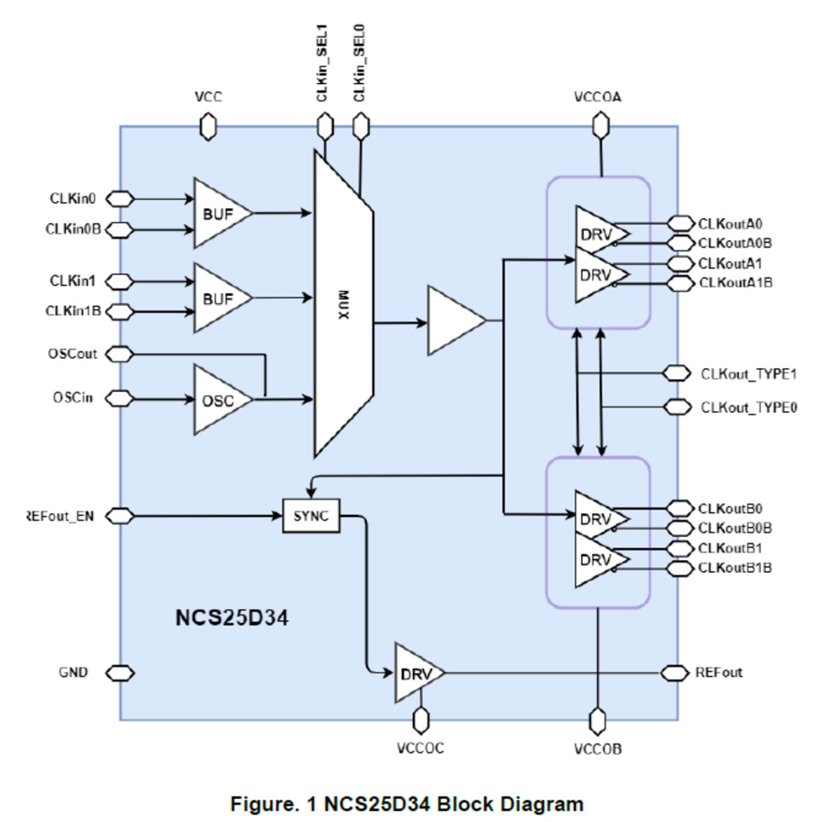
The NCS25D34 is a highly versatile, high-performance, 4-output differential fanout buffer and level translator which can operate up to 3.1GHz with ultra-low additive jitter.
The input clock can be selected from two universal differential or single-ended inputs, or one crystal input which can be overdriven by external single-ended clock. Crystal input frequencies from 8MHz to 50MHz are supported.
A 3:1 input MUX controlled by two external pins is implemented to distribute the selected input clock to two banks of 2 differential outputs and one LVCMOS reference output.
Both banks of differential outputs can be configured as LVPECL, LVDS, HCSL driver mode or disabled mode by two external pins.
The NCS25D34 operates from a 3.3V core supply and 3 independent 3.3V or 2.5V driver output supply, and does not have power supply sequencing requirements between the core and output supply domains.
产品参数
High-performance clock buffer with Ultra-low noise floor of -167 dBc/Hz
• Level translation from 3.3v core supply to output Supply of 3.3V or 2.5V
• 3:1 Input clock multiplexer which is selectable through input pins.
Two universal inputs operate up to 3.1GHz and can accept LVPECL, LVDS, CML, SSTL, HSTL, or HCSL signals
Both differential and single-ended input are supported
Support either DC or AC-coupled input interface
Crystal input frequencies from 8MHz to 50MHz
Crystal overdrive mode with input frequency up to 250MHz
• 4 differential output with two output supply banks
Support LVPECL, LVDS, HCSL or Hi-Z output mode
Ultra-low additive jitter (at 156.25MHz)
40 fs RMS (10K to 20MHz, LVPECL)
52 fs RMS (10K to 20MHz, LVDS)
• Highs PSRR (at 156.25 MHz)-67 dBc LVPECL, -79 dBc LVDS
• LVCMOS reference clock output with independent VCCOC supply and synchronous enable input
Core Supply Voltage(V):3.3V
Output Supply Voltage(V):2.5V, 3.3V
Output frequency(Min)(MHz):-
Output frequency(Max)(MHz):3100
Additive Jitter(fs):43
Temperature Range:-40 to 85
Package:32-pin QFN(5mm x 5mm)
关键词:
集成电路
芯片
半导体
相关产品

产品咨询
客户留言
描述:

北京总公司
北京市朝阳区望京绿地中心A座A区9层
深圳子公司
↵广东省深圳市福田区深南大道6019号金润大厦8层
西安分公司
西安市高新区锦业一路52号宝德云谷国际B座2003
合肥子公司
↵合肥市高新区创新大道2800号创新产业园2期F栋705
电话:+86-551-63657380
新港海岸(北京)科技有限公司